|
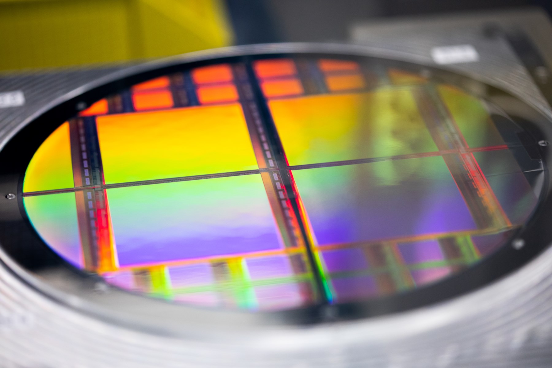
With the ever-decreasing structure sizes in semiconductors, there is a need for an alternative detection of particles or pattern defects.
Optical technologies have become insufficient by nature to detect these nanoscale features due to the limitations of the light wavelengths. This is clearing the way for SEM detection.
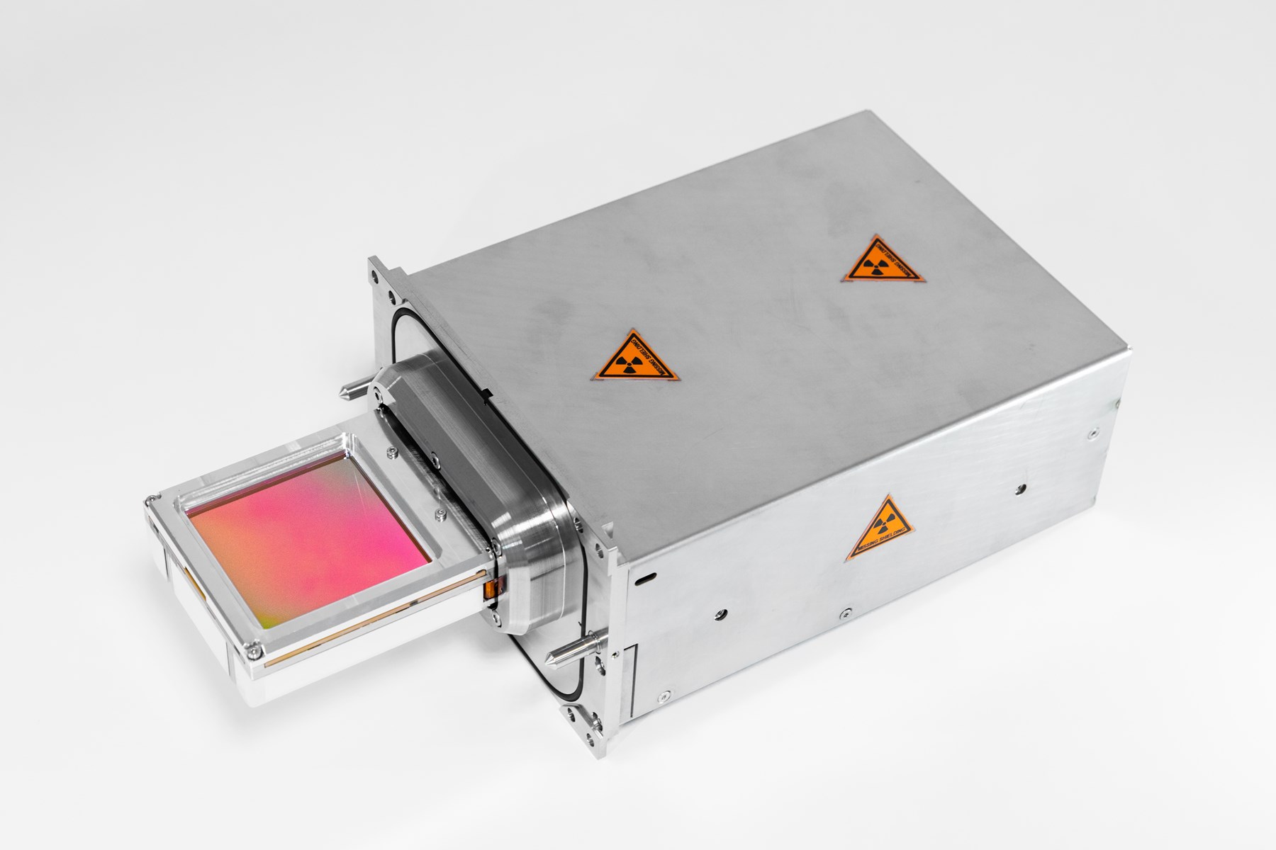
For fast detection of nanoscale features in the semiconductor industry, Prodrive Technologies develops and manufactures advanced multibeam cameras for high-speed imaging to achieve new milestones in sensitivity, resolution, and acquisition speed.
In close cooperation with customers, we define next-generation requirements and set new market standards with our sensor partners. The full development and manufacturing process is covered by us.
Design competencies